Undergraduate researcher Misha Bekeris is the first-author on the newly accepted publication in PSS-RRL, “Rapid Quantification of Nanosphere Lithography Packing Defects Using Scanning Electron Microscopy Edge Effects”. The paper is available for download at: https://doi.org/10.1002/pssr.202000328
Congratulations Misha!
Abstract
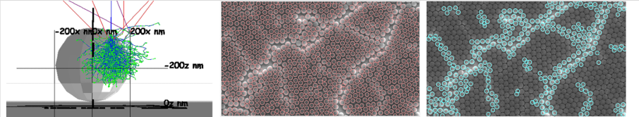
Nanosphere lithography (NSL) is a bottom‐up, self‐assembly approach that enables rapid, low‐cost patterning of nanoscale features. The practical application and scalability of NSL relies on the ability to achieve defect‐free nanosphere self‐assembly over large substrate areas. Self‐assembly methods for single‐layer nanosphere templates are typically evaluated using scanning electron microscopy (SEM) imaging, with literature reports focusing on maximum area of continuous nanosphere coverage. An alternative performance metric—namely, the percentage of nanospheres exhibiting perfect hexagonal close‐packing (%HCP)—is uniquely critical to NSL precision and repeatability. To enhance current methods of evaluating nanosphere self‐assembly, this work presents an SEM image analysis approach for rapidly quantifying packing defects in single‐layer nanospheres to determine %HCP. The method uses variations in SEM edge effect brightness to distinguish spheres with perfect packing from those in defect configurations or along edges. Comparison of image analysis program results with manual counting of nanospheres indicates that the program has a high degree of accuracy, with a mean error on the %HCP metric of +8.6% (absolute error). The results suggest that the present strategy offers a promising pathway to rapid evaluation of nanosphere self‐assembly for high‐precision NSL applications such as surface‐enhanced Raman scattering, photovoltaic cells, and nanogap electrodes.